google-site-verification: google0228a1feb97d321e.html
google-site-verification: google0228a1feb97d321e.html
google-site-verification: google0228a1feb97d321e.html
google-site-verification: google0228a1feb97d321e.html
google-site-verification: google0228a1feb97d321e.html
google-site-verification: google0228a1feb97d321e.html
Semiconductor Industry Spraying Technology -- Semiconductor Industry -- YMUS Ultrasonic Spraying
Semiconductor material as the basis of the whole semiconductor industry chain, semiconductor industry chain can be divided into upper, middle and downstream three sections. Upstream is the semiconductor support industry, composed of semiconductor materials and semiconductor equipment; The midstream is the semiconductor manufacturing industry chain, including the design, manufacturing and spray sealing test of IC, whose products mainly include integrated circuits, components, optoelectronic devices and sensors. Downstream is the specific application field of semiconductors, including consumer electronics, mobile communications, new energy fuel cells, artificial intelligence and other fields. In the semiconductor industry chain, semiconductor materials are located in the upstream of the industry and play a unique role in supporting the industry, which is the bottom foundation of the whole semiconductor industry.
Semiconductor Silicon Wafer
Silicon wafer is the material with the largest amount of semiconductor material. More than 90% of semiconductor products are made of silicon wafer. Silicon wafers can be divided into 6 inch, 8 inch and 12 inch sizes. 8 inch wafers and 12 inch wafers are the mainstream products in the market. Ultra-fine, ultra-clean and ultra-thin silicon wafers have been manufactured by ultrasonic nano-spraying technology.
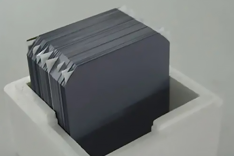
Note:silicon wafer
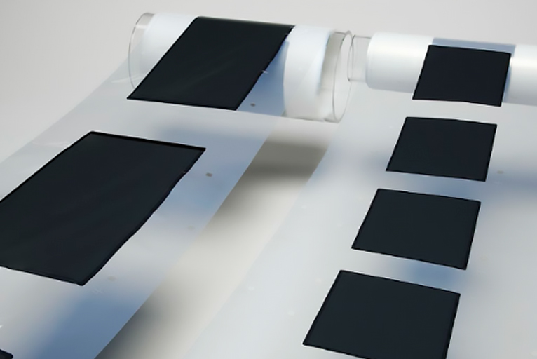
Photoresist Adhesive
Compared with traditional coating processes such as spin coating and penetration coating, ultrasonic spraying technology applied in semiconductor photoresist coating has the advantages of high uniformity, good encapsulation of microstructure and controllable coating area.
Note:Photoresist adhesive
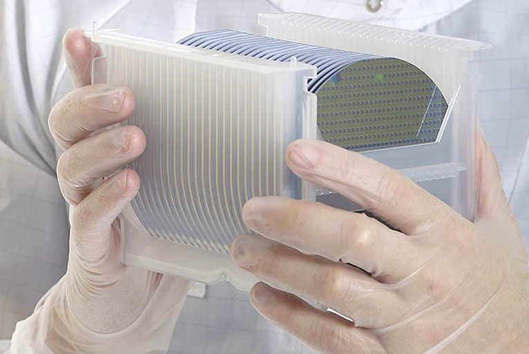
Proton Exchange Membrane
Ultrasonic spraying technology can be used in fuel cells and proton exchange membrane (PEM) electrolytic processes such as Nafion to produce highly durable, uniform coatings of carbon-based catalyst inks that do not deform.
Note:Proton exchange membrane
YMUS ultrasonic spraying equipment can be used in the research and development and production of various nano and sub-micron functional coating films, such as proton exchange membrane fuel cell membrane electrode spraying in the field of new energy, thin film solar cell spraying, such as perovskite solar cells, organic solar cells, transparent conductive film, etc.
