google-site-verification: google0228a1feb97d321e.html
google-site-verification: google0228a1feb97d321e.html
google-site-verification: google0228a1feb97d321e.html
google-site-verification: google0228a1feb97d321e.html
google-site-verification: google0228a1feb97d321e.html
google-site-verification: google0228a1feb97d321e.html
Semiconductor electroluminescence -- LED -- YMUS Ultrasonic spraying
Electroluminescence (EL) is a physical phenomenon that directly converts electrical energy into light energy. From the perspective of luminescence physics, it can be divided into low field electroluminescence and high field electroluminescence. Low field electroluminescence generally refers to the injection of a few carriers on the PN junction of Group III-V compound to produce the luminescence caused by recombination, which is the common light emitting diode (LED). High field electroluminescence is a kind of luminescence of high field non-junction device, which is made of II-VI compound.
High field electroluminescence devices can be divided into three types: thin film type, thick film mixed type and powder type. Ac film type and hybrid type can be used as matrix display, which is the main aspect of the development of EL technology. Ac powder type is used for flat light sources such as LCD.
Ac thin film electroluminescent display is an all-solid flat panel display device with a series of properties unique to solid devices:
1, the response speed is fast, up to tens of microseconds.
2, the Angle of view is large, up to ±80°, can be watched by many people at the same time.
3, wide range of working temperature, -55℃~+125℃, more than the general integrated circuit can withstand the extreme working temperature.
4, thin and firm, effective device itself has no cavity and sealing structure, can withstand the glass plate can withstand a variety of vibration and impact conditions.
Currently, semiconductor electroluminescence mainly has three directions: LED (semiconductor electroluminescence), OLED (semiconductor material electroluminescence), and QLED (inorganic semiconductor quantum dot film electroluminescence).

Note:Semiconductor electroluminescence
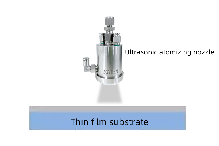
Preparation of Inorganic Quantum Dot Electroluminescent Devices (QLEDs) by YMUS Ultrasonic Atomizing Spraying Technology
Compared with the conventional spin coating process, ultrasonic spraying technology has three advantages:
1. It saves materials. For the ordinary spinning coating process, more than 90% of the materials are wasted in the spinning coating process, while the material utilization rate in the spraying process is up to 95%.
2.Spraying process can realize the preparation of large area devices, but spinning coating technology is not. This makes spin coating technology can not be applied to industrial production;
3. The common spin coating technology cannot mask the device to achieve the preparation of pixels, while the spraying technology is fully compatible with the mask process.
YMUS spray technology is a low-cost and efficient solution based film preparation process, which has been used in industrial production.
AFM diagram of different thickness:
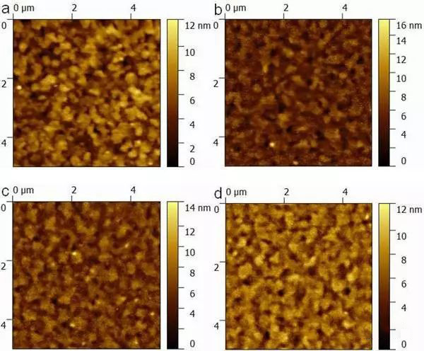
(a) Surface morphology of NiO after deposition of Al2O3 layers of different thickness;
(b) 2nm; (c) 5nm; (d) 8nm.
YMUS has prepared inorganic quantum dot electroluminescent devices (QLEDs) using ultrasonic atomization spraying technology, which has played an excellent role in promoting the development of inorganic QLED devices. Ymus has improved the technical service for the preparation of high quality Qleds.
