google-site-verification: google0228a1feb97d321e.html
google-site-verification: google0228a1feb97d321e.html
google-site-verification: google0228a1feb97d321e.html
google-site-verification: google0228a1feb97d321e.html
google-site-verification: google0228a1feb97d321e.html
google-site-verification: google0228a1feb97d321e.html
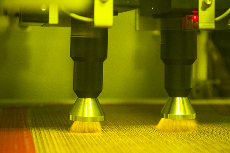
Plasma cleaning has a wide range of application prospects in microelectronics packaging. The successful application of plasma cleaning technology depends on the optimization of process parameters, including process pressure, plasma excitation frequency and power, time and process gas type, reaction chamber and electrode configuration and the position of workpiece to be cleaned, etc. In the back production process of semiconductor, due to the fingerprint, daming aid, solder, scratch, stain, fine dust, resin residue, autothermal oxidation, organic matter, etc., the surface of devices and materials form famous stains, these stains will obviously affect the packaging production and product quality, the use of plasma cleaning technology, can easily remove these molecular level pollution formed in the production process, Thus, the manufacturability, reliability and yield of the package can be significantly improved.
