google-site-verification: google0228a1feb97d321e.html
google-site-verification: google0228a1feb97d321e.html
google-site-verification: google0228a1feb97d321e.html
google-site-verification: google0228a1feb97d321e.html
google-site-verification: google0228a1feb97d321e.html
google-site-verification: google0228a1feb97d321e.html
YMUS Ultrasonic Spraying technology for MEMS -- Semiconductor Industry
With the development of microelectromechanical systems (MEMS), it is necessary to cover conformal photoresist on uneven surfaces with channels, V-grooves, and deep holes in order to meet the evolving requirements of small size and high integration devices. Silicon through-hole technology (TSV) is an important technology in 3D-IC packaging. Through the vertical interconnection of chip to chip and wafer to wafer, high quality chips with high stack density, small size, fast running speed and low power consumption can be obtained. Therefore, there is an increasing demand for coating photoresist to TSV structure with uneven morphology, which promotes the development of new coating photoresist technology.
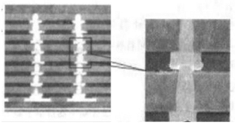
Note:SEM images were encapsulated with TSV 3D-IC technology
The rotary coating process is the most traditional coating process, but due to the effect of centrifugal force and gravity on the photoresist during the spinning process, the conventional rotary coating technology can not achieve conformal photoresist coating on the surface of these morphologic wafers. The optimized electron beam deposition photoresist technology can achieve conformal photoresist coverage. However, in this process, a conductive coating is required as the base layer. This conductive coating is unfavorable to the post-process, and the cost is relatively high. In order to satisfy this conformal photoresist coating, a new ultrasonic spraying technology emerged. This ultrasonic spraying technology has the characteristics of simple operation, economy, high repeatability, and has the tendency to replace the conventional spin coating technology. YMUS ultrasonic spraying technology is a key part of its use of ultrasonic atomizing nozzle. Compared with electron beam deposition photoresist, ultrasonic spraying technology greatly saves cost.
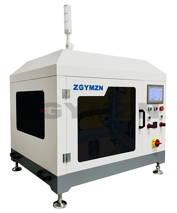
YMUS-ZM200 Ultrasonic spraying equipment
Experimental test:
The ultrasonic nozzle is composed of a liquid inlet part, a connecting controller part, a transducer and a nozzle. The ultrasonic nozzle converts part of the high-frequency electrical energy into mechanical energy through the transducer, which is transferred to the liquid to generate standing waves. As the liquid leaves the atomized surface of the nozzle, it is broken into a fine mist of uniform micron-sized droplets.
Ultrasonic spraying application:
◆ New energy: fuel cell, film electrode, film solar cell, exchange film, etc.
◆ Medical treatment: balloon catheter, blood vessel injector, stent, biosensor, microfluidic chip, etc.
◆ Microelectronics semiconductor electronics: flux, photoresist coating, conductive coating, hydrophilic coating, etc.
◆ Glass production: glass coating, float glass, photovoltaic glass, photoresist film, transparent conduction, etc.;
◆ Nanotechnology: carbon nanotubes, polymer fibers, nano films, etc.;
