google-site-verification: google0228a1feb97d321e.html
google-site-verification: google0228a1feb97d321e.html
google-site-verification: google0228a1feb97d321e.html
google-site-verification: google0228a1feb97d321e.html
google-site-verification: google0228a1feb97d321e.html
google-site-verification: google0228a1feb97d321e.html
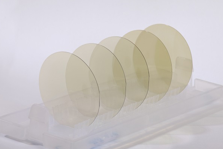
The core of silicon carbide substrate -- crystal growth -- YMUS Ultrasonic spray
The performance of silicon carbide material breaks through the limit of silicon based devices. Compared with traditional silicon based devices, the power density, switching efficiency and device loss of silicon carbide power devices have been greatly optimized. The production process of SIC products starts from the preparation of material end substrate and epitaxial, goes through the design and manufacture of chips, and then to the packaging of modules, and finally flows to the downstream application market. From the point of view of cost breakdown, substrate cost accounts for 46%, is the most core link in the industrial chain. At present, in the substrate preparation link, the crystal growth link, affected by the slow growth rate of silicon carbide crystal, black box operation and many types of silicon carbide crystal structure, resulting in small yield of silicon carbide substrate, low yield; In the process of cutting grinding and polishing, because silicon carbide is a brittle material with high hardness, the processing difficulty of cutting grinding and polishing is increased, the material utilization rate of silicon carbide crystal column is low, and the number of output wafers is less. The above difficulties cause the high cost of silicon carbide preparation and become the bottleneck restricting the development of the industry. In the future, with the increase of substrate size from 6 "to 8", continuous optimization of yield and related production cutting and polishing process upgrading, the cost of silicon carbide material is expected to decrease significantly, which will effectively reduce the overall device price, improve the replacement willingness of downstream customers, and pull up the market penetration of silicon carbide power devices.
1, Improve the crystal growth link
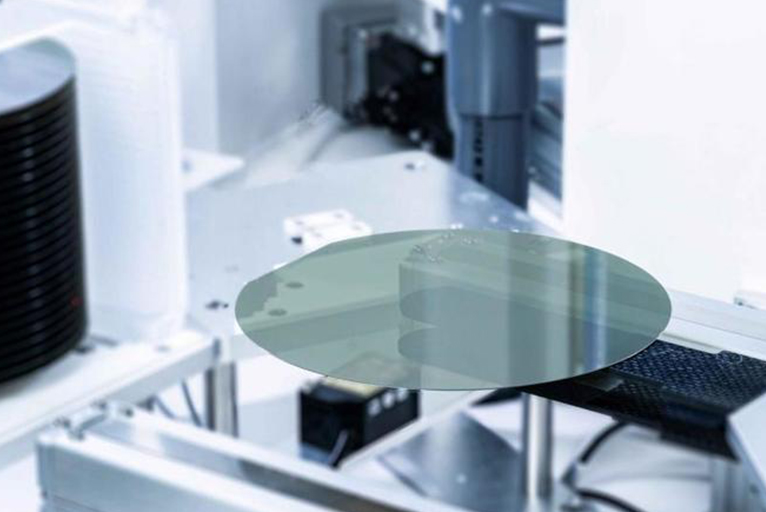
YMUS ultrasonic spraying technology in the crystal growth, after accurate calculation and adjustment, the temperature, solution concentration and flow rate of the crystal growth process can be precisely controlled, to ensure the growth of crystal uniformity and continuity. In addition, ultrasonic spraying technology can be used to evenly mix various solutes in the crystal growth area, so that more uniform, more regular crystals can be grown.
2, Improve the grinding and polishing link
YMUS ultrasonic dispersion liquid supply technology can evenly add various powders, nanoparticles, oxides and other particles to the liquid for mixing, forming a mixture with higher physical and chemical properties. The dispersion efficiency is high and the speed is fast. The micro particles can be mixed into submicron level to obtain more stable surface quality. In the process of wafer grinding and polishing, the ultrasonic dispersion technology can effectively disperse the silicon metal particles into the solution, so that the liquid distribution is uniform, which enhances the performance characteristics and improves the process stability in the process of forming and cutting.
YMUS-ZS400 Fully automatic, programmable stand-alone system with coordinated XYZ motion control, multifunctional medium to high volume or pilot scale production of film coatings using Windows-based software and user-friendly demonstrator with trackball. Standard conveyors can be configured for on-line coating solutions.
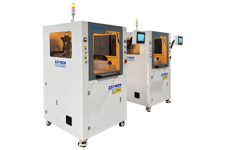
YMUS-ZS400 ultrasonic spraying machine
