google-site-verification: google0228a1feb97d321e.html
google-site-verification: google0228a1feb97d321e.html
google-site-verification: google0228a1feb97d321e.html
google-site-verification: google0228a1feb97d321e.html
google-site-verification: google0228a1feb97d321e.html
google-site-verification: google0228a1feb97d321e.html
The king of SiC third generation semiconductor substrate material - semiconductor material - YMUS ultrasonic spraying
In recent years, China's electronic information products have developed at a remarkable speed, and the industrial scale has become China's first pillar industry. Semiconductor materials and applications have become an important symbol to measure a country's economic development, scientific and technological progress and national defense strength. In the development of semiconductor industry, silicon and germanium are called the first generation semiconductor materials; Gallium arsenide, phosphide occlusion, gallium phosphide, arsenide occlusion, aluminum arsenide and their alloys are called the second generation semiconductor materials. Gallium nitride, silicon carbide, zinc selenide and diamond with wide band gap (Eg>2.3eV) are called the third generation semiconductor materials. Among them, silicon carbide and gallium nitride are the semiconductor materials with the most clear commercial prospects at present, and the new generation of "leaders" in the semiconductor industry.
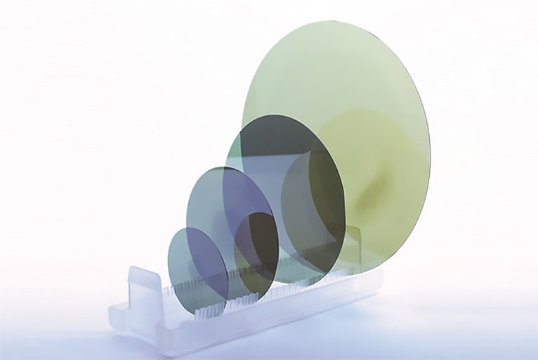
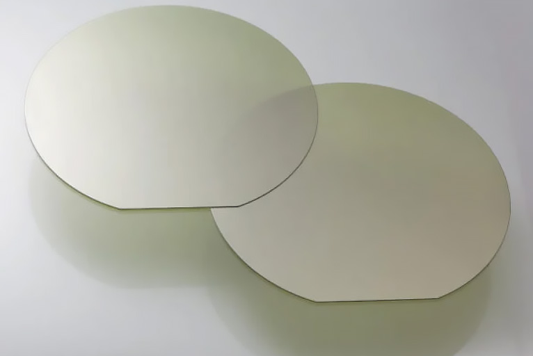
Silicon Carbide Substrate (Silicon Carbide Substrate) is a substrate used to make silicon carbide devices. It is a sheet substrate made of silicon carbide material that can be used as a supporting substrate for semiconductor devices.
Silicon carbide has a high thermal conductivity, which means that the silicon carbide substrate can effectively conduct heat and maintain a uniform temperature distribution of the device, thereby improving the stability and reliability of the device. Silicon carbide substrate has a high breakdown electric field strength and can withstand higher electric fields, thus providing a higher operating voltage range. This is important for some high-voltage applications, such as power electronics and electric vehicle drive systems. Excellent crystal quality: The development of silicon carbide substrate preparation process has made it possible to obtain high-quality silicon carbide crystals with lower defect density and higher crystal structure integrity, which is conducive to the preparation of high-performance devices.
Silicon carbide substrate has a wide range of applications, mainly concentrated in high power electronics, optoelectronics, sensors, high temperature electronics and other fields. Silicon carbide substrate can also be used as a substrate for other materials, such as silicon nitride and aluminum nitride. It should be noted that due to the relatively complex preparation process of silicon carbide substrate, the cost is high. However, with the advancement of technology and the promotion of large-scale production, the price of silicon carbide substrate is expected to gradually decrease, and further promote the development and application of silicon carbide devices.
The silicon carbide crystal film is prepared by YMUS ultrasonic spraying technology, which makes the crystal deposition uniform and improves the consistency of the grown film. Ultrasonic spraying silicon carbide seed crystal growth method is of great significance in the preparation and research of silicon carbide devices, and can be used to prepare silicon carbide thin films, nanoparticles, etc., and has a wide range of applications in new energy, optoelectronics, power electronics, sensors, biomedicine and other fields.
